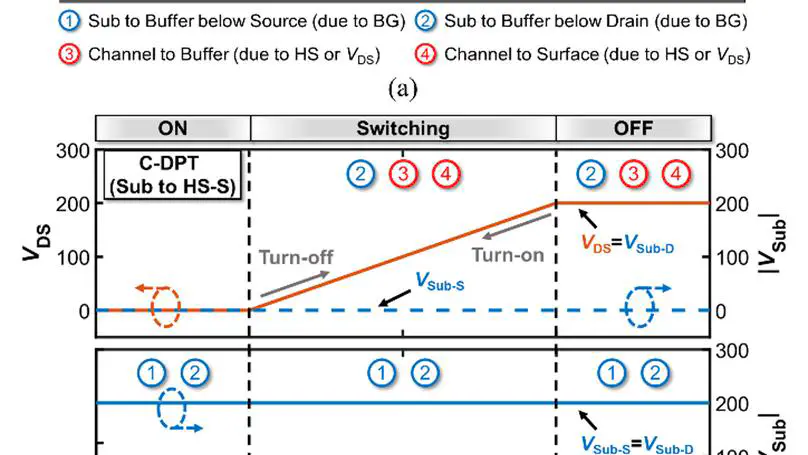
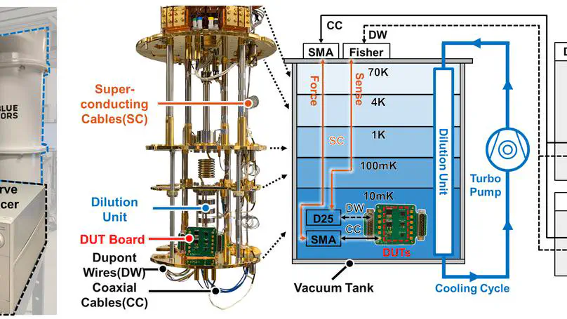
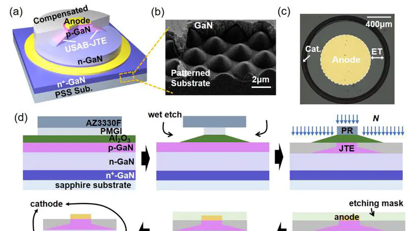
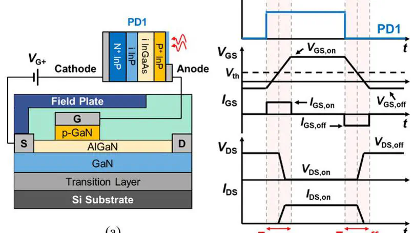
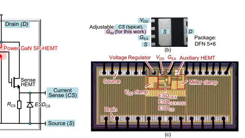
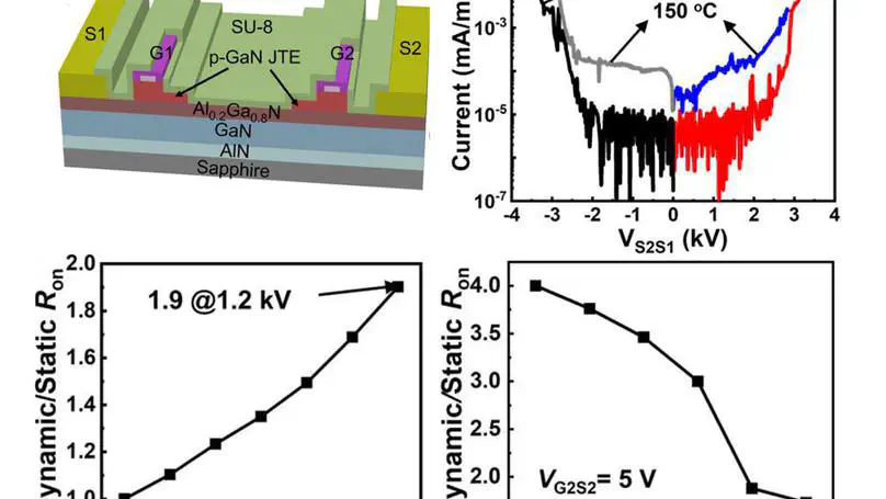
Our group mainly explores wide-bandgap (WBG) and ultra-wide bandgap (UWBG) materials, devices, and circuits for next-generation electronics applications. Our current research focuses on a few major areas: (1) WBG semiconductors for power and RF electronics; (2) Power device reliability and robustness, packaging, circuit-level integration, and system-level applications; (3) Machine learning assisted material-device-circuit co-design; (4) WBG and UWBG materials and devices for electronic, photonic, biological and quantum applications; (5) Devices, circuits and systems for extreme environment applications.
Our group mainly published in the communities of Electron Devices and Power Electronics. Here is a sketch of the group's major corresponding-authored papers till Aug. 2025.
We typically have openings for PhD students, postdoctoral researchers, and visiting scholars with backgrounds in cleanroom fabrication, semiconductor devices, and power electronics circuits. Most PhD students admitted to our group have prior publications in the relevant fields. If you are interested, please contact Professor Yuhao Zhang. Although the peak PhD application season is from September to December, we accept applications year-round. We provide full financial support to all PhD students and also assist with applications to the Hong Kong PhD Fellowship Scheme and the HKU Presidential PhD Scholar Programme.
Related Links:
Our group mainly published in the communities of Electron Devices and Power Electronics. Here is a sketch of the group's major corresponding-authored papers till Aug. 2025.
- Electron Devices: IEDM (21), ISPSD (12), IRPS (7), IEEE Electron Device Lett. (21), Appl. Phys. Lett. (14), IEEE Trans. Electron Devices (16)
- Power Electronics: IEEE Trans. Power Electronics (21), IEEE J. Emerg. Sel. Top. Power Electron. (3), APEC (16), ECCE (7)
- Broad Fields: Nat. Electron. (1), Nat. Commun. (1), Nat. Rev. Electr. Eng. (1), Adv. Mater. (1)
We typically have openings for PhD students, postdoctoral researchers, and visiting scholars with backgrounds in cleanroom fabrication, semiconductor devices, and power electronics circuits. Most PhD students admitted to our group have prior publications in the relevant fields. If you are interested, please contact Professor Yuhao Zhang. Although the peak PhD application season is from September to December, we accept applications year-round. We provide full financial support to all PhD students and also assist with applications to the Hong Kong PhD Fellowship Scheme and the HKU Presidential PhD Scholar Programme.
Related Links:
Selected Publications:
Major Awards of the Group:
- Y. Qin, Z. Yang, H. Gong, A. Jacobs, J. Spencer, M. Porter, B. Wang, K. Sasaki, C-H. Lin, M. Tadjer, and Y. Zhang*, “10 kV, 250 oC Operational, Enhancement-Mode Ga2O3 JFET with Charge-Balance and Hybrid-Drain Designs,” 2024 IEEE International Electron Devices Meeting (IEDM), Dec. 2024 (selected as the IEDM Technical Highlight)
- X. Yang, R. Zhang, Q. Yang, Q. Song, E. Litchford, A. J. Walker, S. Pidaparthi, C. Drowley, D. Dong, Q. Li, and Y. Zhang*, “Evaluation and MHz Converter Application of 1.2-kV Vertical GaN JFET,” IEEE Transactions on Power Electronics, vol. 39, no. 12, pp. 15720–15731, Dec. 2024.
- M. Xiao, Y. Wang, R. Zhang, Q. Song, M. Porter, E. Carlson, K. Cheng, K. Ngo, and Y. Zhang*, “Robust Avalanche in 1.7 kV Vertical GaN Diodes With a Single-Implant Bevel Edge Termination,” IEEE Electron Device Letters, vol. 44, no. 10, pp. 1616–1619, Oct. 2023. (2023 IEEE George Smith Award)
- Y. Zhang*, F. Udrea*, and H. Wang*, “Multidimensional device architectures for efficient power electronics,” Nature Electronics, vol. 5, no. 11, Nov. 2022.
- Xiao, Y. Ma, Z. Du, V. Pathirana, K. Cheng, A. Xie, E. Beam, Y. Cao, F. Udrea, H. Wang, and Y. Zhang*, “Multi-Channel Monolithic-Cascode HEMT (MC2-HEMT): A New GaN Power Switch up to 10 kV,” 2021 IEEE International Electron Devices Meeting (IEDM), Dec. 2021. (selected as the IEDM Technical Highlight, covered by Nature Electronics).
Major Awards of the Group:
- 2025 Yuhao Zhang, HE Research Fellowship by HE Science Foundation
- 2025 Yuhao Zhang, Young Scientist Award of the Compound Semiconductor Week for “Significant contributions to wide-bandgap and ultra-wide-bandgap power devices with pioneering demonstrations of multidimensional devices – superjunction, multi-channel, and FinFET – in GaN and Ga2O3.”
- 2025 Joseph Kozak (alumina), Richard M. Bass Outstanding Young Power Electronics Engineer Award
- 2025 Qihao Song and Xin Yang, 2025 APEC Best Presentation Awards
- 2024 IEDM Technical Highlight of the 2024 70th IEEE International Electron Devices Meeting (IEDM)
- 2024 46th JSAP (Japanese Society of Applied Physics) Award for Best Review Paper (only one awardee each year in all JSAP journals)
- 2024 IEEE E. George Smith Award for the best paper of the year in IEEE Electron Devices Letters (only one awardee each year)
- 2024 Yuhao Zhang, Office of Naval Research (ONR) Young Investigator Program (YIP) Award
- 2023 Ruizhe Zhang, APEC Best Presentation Award
- 2022 Yuhao Zhang, Faculty Fellow Award of Virginia Tech Engineering
- 2021 IEDM Technical Highlight of the 2021 67th IEEE International Electron Devices Meeting
- 2021 Yuhao Zhang, National Science Foundation CAREER Award
- 2021 Yuhao Zhang, Outstanding Assistant Professor Award of Virginia Tech Engineering
- 2021 Joseph Kozak, Ph. D. Thesis Talk Award of the IEEE Power Electronics Society (5 awardees each year in the world)
- 2021 Qihao Song, APEC Best Presentation Award 2021
- 2020 IEDM Technical Highlight of the 2020 66th IEEE International Electron Devices Meeting (IEDM)
- 2019 IEEE E. George Smith Award for the best paper of the year in IEEE Electron Devices Letters (only one awardee each year)
- 2017 Yuaho Zhang, MIT Microsystems Technology Laboratories Best Doctoral Dissertation Award
📑 Journal Papers/Articles
Our newest journal papers
📰 Conference Papers
Our newest conference papers
© 2025 Prof. Yuhao Zhang at Wide Bandgap Electronics Group | Department of EEE | HKU | Built with CC BY NC ND 4.0
