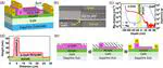
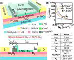
Researchers based in the USA, China and the UK have reported 10kV performance from enhancement (E)-mode gallium nitride (GaN) high-electron-mobility transistors (HEMTs) with a standard highly doped p-GaN gate. The p-GaN layer used for the gate also allowed construction of a reduced-surface-field (RESURF) structure to massage the electric (E)-field for access of greater breakdown voltages. The 10kV GaN HEMT had a 69mΩ-cm2 specific on-resistance (RON,SP), which is lower than reported silicon carbide (SiC) metal-oxide-semiconductor field-effect transistors (MOSFETs) with the same voltage rating.
Aug 28, 2025 · Semiconductor Today