First Characterization of Si IGBT, SiC MOSFET, and GaN HEMT at Deep Cryogenic Temperatures down to 10 Millikelvins
Abstract
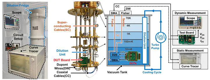
Electrical energy conversion at deep cryogenic temperatures (T < 4.2 K) is highly desirable for applications in space exploration, quantum computing, biomedical imaging, and emerging power delivery systems. However, the operational viability of power semiconductor devices in this temperature regime remains largely unexplored. Notably, no prior studies have reported high-voltage or dynamic switching characteristics of GaN and SiC power devices below 77 K. In this work, we present the first comprehensive characterization of the static and dynamic performance of Si IGBT, SiC MOSFET, and GaN HEMT devices down to 10 mK. A cryogen-free dilution refrigerator, originally designed for quantum physics experiments, is adapted for power device testing by integration with a custom circuit setup for double-pulse testing (DPT) and dynamic on-resistance (RON) test. At T < 1 K, all three devices are found to retain the normally-off operation, high breakdown voltage, and the capability of hardswitching under gate control. GaN HEMTs demonstrate the absence of dynamic RON degradation, with RON decreasing by 4 times compared to room temperature. This can be explained by the trap freeze-out and increased channel mobility. Differently, SiC MOSFET becomes non-Ohmic below ∼60 K. The knee voltages (VK) of SiC MOSFET and Si IGBT both increase at lower temperatures, leading to elevated conduction loss. The sustained current conduction and high VK in lowly-doped SiC and Si drift layers, despite carrier freeze-out, can be explained by the shallowlevel impact ionization with donor states. These findings lay the foundation for developing deep cryogenic power electronics at temperatures below the current operational boundaries.