ß-Ga2O3 Junction Barrier Schottky (JBS) Diodes with Sputtered p-Type NiO (pending)
Abstract
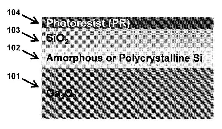
A self-aligned lithography process for the fabrication of an electronic device having predefined areas of a second semiconductor material having a second conductivity type deposited into trenches formed in a first semiconductor material layer having a first conductivity type. A single lithography mask is used for etching trenches in the first semiconductor material, enabling cleaning of the trenches, and providing defined areas for the deposition of the second semiconductor material into the first semiconductor material. The presence of the areas of the second semiconductor material within the first semiconductor material creates a heterojunction beneath a metal for the formation of a first type of contact to the first semiconductor material and a second type of contact to the second type of material. By using a single mask for the etching, cleaning, and filling steps, misalignment issues plaguing devices having small (1-2 μm) feature sizes is eliminated.